- 您现在的位置:买卖IC网 > Sheet目录2006 > LTC2435CGN#TRPBF (Linear Technology)IC ADC DIFF I/REF 20BIT 16-SSOP
LTC2435/LTC2435-1
15
24351fc
For more information www.linear.com/LTC2435
applicaTions inForMaTion
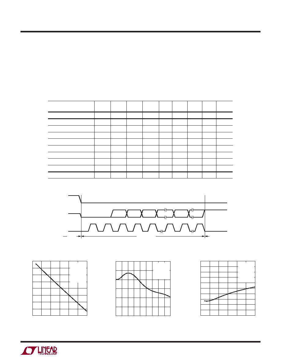
While the variation in offset with supply voltage is propor-
tional to VCC (see Figure 4), several characteristics of this
variation can be used to eliminate the effects. First, the
variation with respect to supply voltage is linear. Second,
themagnitudeoftheoffseterrordecreaseswithdecreased
supply voltage. Third, the offset error in microvolts is al-
most independent with reference and therefore the offset
in ppm is inverse proportional to reference voltage. As a
result, by tying VCC to VREF , the variation with supply can
be reduced, see Figure 6. The variation with supply is less
than 15ppm over the entire 2.7V to 5.5V supply range.
Table 2. LTC2435/LTC2435-1 Output Data Format
Differential Input Voltage
VIN*
Bit 23
EOC
Bit 22
DMY
Bit 21
SIG
Bit 20
MSB
Bit 19 Bit 18
Bit 17
…
Bit 0
VIN* ≥ 0.5 VREF**
0
1
0
…
0
0.5 VREF** – 1LSB
0
1
0
1
…
1
0.25 VREF**
0
1
0
1
0
…
0
0.25 VREF** – 1LSB
0
1
0
1
…
1
0
1
0
…
0
–1LSB
0
1
…
1
–0.25 VREF**
0
1
0
…
0
–0.25 VREF** – 1LSB
0
1
0
1
…
1
–0.5 VREF**
0
1
0
…
0
VIN* < –0.5 VREF**
0
1
…
1
*The differential input voltage VIN = IN+ – IN–.
**The differential reference voltage VREF = REF+ – REF–.
Figure 3. Output Data Timing
MSB
SIG
“0”
BIT 0
BIT 19
BIT 5
LSB
BIT 20
BIT 21
BIT 22
SDO
SCK
CS
EOC
BIT 23
SLEEP
DATA OUTPUT
CONVERSION
2435 F03
Hi-Z
Figure 4. Offset vs VCC
Figure 6. Offset vs VCC (VREF = VCC)
Figure 5. Offset vs Temperature
VCC (V)
2.5
3.0
OFFSET
ERROR
(ppm
OF
V
REF
)
3.5
4.5
4.0
5.0
5.5
2435 F04
–350
–400
–450
–500
–550
–600
–650
–700
–750
REF+ = 2.5V
REF– = GND
VIN = 0V
VINCM = GND
FO = GND
TA = 25°C
TEMPERATURE (°C)
–45 –30
0
OFFSET
ERROR
(ppm
OF
V
REF
)
–15
15 30
90
2435 F05
45 60 75
–324
–325
–326
–327
–328
–329
–330
VCC = 5V
VREF = 5V
VIN = 0V
VINCM = GND
FO = GND
VCC and VREF (V)
2.5
3.0
OFFSET
ERROR
(ppm
OF
V
REF
)
3.5
4.5
4.0
5.0
5.5
2435 F06
–300
–305
–310
–315
–320
–325
–330
–335
–340
–345
–350
REF+ = VCC
REF– = GND
VIN = 0V
VINCM = GND
FO = GND
TA = 25°C
–
发布紧急采购,3分钟左右您将得到回复。
相关PDF资料
LTC2442IG#PBF
IC ADC 24BIT 4CH 36-SSOP
LTC2446IUHF#TRPBF
IC ADC 24BIT 8CH HI SPEED 38QFN
LTC2448IUHF#TRPBF
IC ADC 24BIT HI SPEED 38QFN
LTC2451ITS8#TRPBF
IC ADC 16BIT DELTA SIG TSOT23-8
LTC2452ITS8#TRPBF
IC ADC 16BIT DELTA SIG TSOT23-8
LTC2453ITS8#TRMPBF
IC ADC 16BIT DELTA SIG TSOT23-8
LTC2482IDD#TRPBF
IC ADC 16BIT 10-DFN
LTC2483IDD#TRPBF
IC ADC 16BIT I2C 10-DFN
相关代理商/技术参数
LTC2435IGN
功能描述:IC CONV A/D 20BIT DIFF 16-SSOP RoHS:否 类别:集成电路 (IC) >> 数据采集 - 模数转换器 系列:- 标准包装:2,500 系列:- 位数:16 采样率(每秒):15 数据接口:MICROWIRE?,串行,SPI? 转换器数目:1 功率耗散(最大):480µW 电压电源:单电源 工作温度:-40°C ~ 85°C 安装类型:表面贴装 封装/外壳:38-WFQFN 裸露焊盘 供应商设备封装:38-QFN(5x7) 包装:带卷 (TR) 输入数目和类型:16 个单端,双极;8 个差分,双极 配用:DC1011A-C-ND - BOARD DELTA SIGMA ADC LTC2494
LTC2435IGN#PBF
功能描述:IC ADC DIFF I/REF 20BIT 16-SSOP RoHS:是 类别:集成电路 (IC) >> 数据采集 - 模数转换器 系列:- 标准包装:2,500 系列:- 位数:16 采样率(每秒):15 数据接口:MICROWIRE?,串行,SPI? 转换器数目:1 功率耗散(最大):480µW 电压电源:单电源 工作温度:-40°C ~ 85°C 安装类型:表面贴装 封装/外壳:38-WFQFN 裸露焊盘 供应商设备封装:38-QFN(5x7) 包装:带卷 (TR) 输入数目和类型:16 个单端,双极;8 个差分,双极 配用:DC1011A-C-ND - BOARD DELTA SIGMA ADC LTC2494
LTC2435IGN#TR
功能描述:IC CONV A/D 20BIT DIFF 16-SSOP RoHS:否 类别:集成电路 (IC) >> 数据采集 - 模数转换器 系列:- 标准包装:1,000 系列:- 位数:16 采样率(每秒):45k 数据接口:串行 转换器数目:2 功率耗散(最大):315mW 电压电源:模拟和数字 工作温度:0°C ~ 70°C 安装类型:表面贴装 封装/外壳:28-SOIC(0.295",7.50mm 宽) 供应商设备封装:28-SOIC W 包装:带卷 (TR) 输入数目和类型:2 个单端,单极
LTC2435IGN#TRPBF
功能描述:IC ADC DIFF I/REF 20BIT 16-SSOP RoHS:是 类别:集成电路 (IC) >> 数据采集 - 模数转换器 系列:- 标准包装:1,000 系列:- 位数:16 采样率(每秒):45k 数据接口:串行 转换器数目:2 功率耗散(最大):315mW 电压电源:模拟和数字 工作温度:0°C ~ 70°C 安装类型:表面贴装 封装/外壳:28-SOIC(0.295",7.50mm 宽) 供应商设备封装:28-SOIC W 包装:带卷 (TR) 输入数目和类型:2 个单端,单极
LTC2436-1CGN
功能描述:IC ADC 2CH DIFF-IN 16BIT 16SSOP RoHS:否 类别:集成电路 (IC) >> 数据采集 - 模数转换器 系列:- 标准包装:2,500 系列:- 位数:16 采样率(每秒):15 数据接口:MICROWIRE?,串行,SPI? 转换器数目:1 功率耗散(最大):480µW 电压电源:单电源 工作温度:-40°C ~ 85°C 安装类型:表面贴装 封装/外壳:38-WFQFN 裸露焊盘 供应商设备封装:38-QFN(5x7) 包装:带卷 (TR) 输入数目和类型:16 个单端,双极;8 个差分,双极 配用:DC1011A-C-ND - BOARD DELTA SIGMA ADC LTC2494
LTC2436-1CGN#PBF
功能描述:IC ADC 2CH DIFF-IN 16BIT 16SSOP RoHS:是 类别:集成电路 (IC) >> 数据采集 - 模数转换器 系列:- 标准包装:1 系列:microPOWER™ 位数:8 采样率(每秒):1M 数据接口:串行,SPI? 转换器数目:1 功率耗散(最大):- 电压电源:模拟和数字 工作温度:-40°C ~ 125°C 安装类型:表面贴装 封装/外壳:24-VFQFN 裸露焊盘 供应商设备封装:24-VQFN 裸露焊盘(4x4) 包装:Digi-Reel® 输入数目和类型:8 个单端,单极 产品目录页面:892 (CN2011-ZH PDF) 其它名称:296-25851-6
LTC2436-1CGN#TR
功能描述:IC CONV A/D 16B 2CH DIFF 16SSOP RoHS:否 类别:集成电路 (IC) >> 数据采集 - 模数转换器 系列:- 标准包装:2,500 系列:- 位数:16 采样率(每秒):15 数据接口:MICROWIRE?,串行,SPI? 转换器数目:1 功率耗散(最大):480µW 电压电源:单电源 工作温度:-40°C ~ 85°C 安装类型:表面贴装 封装/外壳:38-WFQFN 裸露焊盘 供应商设备封装:38-QFN(5x7) 包装:带卷 (TR) 输入数目和类型:16 个单端,双极;8 个差分,双极 配用:DC1011A-C-ND - BOARD DELTA SIGMA ADC LTC2494
LTC2436-1CGN#TRPBF
功能描述:IC CONV A/D 16B 2CH DIFF 16SSOP RoHS:是 类别:集成电路 (IC) >> 数据采集 - 模数转换器 系列:- 标准包装:2,500 系列:- 位数:16 采样率(每秒):15 数据接口:MICROWIRE?,串行,SPI? 转换器数目:1 功率耗散(最大):480µW 电压电源:单电源 工作温度:-40°C ~ 85°C 安装类型:表面贴装 封装/外壳:38-WFQFN 裸露焊盘 供应商设备封装:38-QFN(5x7) 包装:带卷 (TR) 输入数目和类型:16 个单端,双极;8 个差分,双极 配用:DC1011A-C-ND - BOARD DELTA SIGMA ADC LTC2494